

 Somewhere on these pages, I wrote that when it comes to RF, only a dead probe is a good probe. I still mean it. The good old approach with a tip and and an alligator clip is simply useless above ca. 100Mhz. The impedance of your probe (e.g., 10pf for a 500MHz Keysight passive probe), plus the inductance of the ground connection will distort your fast, nanosecond-risetime signal to a degree where measurements turn to guesswork. What RF or subnanosecond switching stuff really needs are planned, impedance matched tap points in your circuit where you can attach a 50Ohm scope channel and then see what is going on without loading, detuning or even disabling the circuit you want to measure.
The measurement equipment industry would just love to sell you some probes specified until a few GHz and costing a fortune (several k€). A 2GHz probe could come with, say, 0.5pF of capacitive loading, and a voltage range of just a few volts, the faster the fewer. At 2 GHz, 0.5pF are around 160Ohms of loading. Now imagine touching a high impedance point with something like that, or a part of a filter or oscillator tank – just forget about that. In my opinion, probes like that are for digital use only, or, at best, in low impedance circuitry where level accuracy or risetime deterioration is unimportant. When you look at the probe tip geometry of these probes, I have extreme doubts about the repeatability and accuracy of measurements obtained in GHz frequency ranges. Maybe I am too conservative, but in my opinion there simply are no precision RF measurements using probes (*).
So, what if you want to measure some point in a circuit that cannot reasonably be tapped into a 50Ohm output ? Say, you want to see the bridge center point of a varactor amplifier, how would you do that ? (I admit this is an extreme case).
What would be needed is something like that:
- Input impedance: 0.3pF or even less (this is probably very hard to do)
- Frequency range 100kHz to a few 100MHz, to 1GHz if possible
- Voltage range up to 5Vpp
- Solderable into the circuit (or how else could you keep coupling capacitance low ?) with very short leads. No clips or other undefined impedance stuff.
- ca. 20dB power attenuation. This is unimportant, as it can be calibrated out later.
Simple math reveals that there is no possible solution for a purely passive probe. Even if we divide 1:100, we end up with 30pF of total capacitance including the cable and scope input (10pF). For 1:10, the situation is even more hopeless. So what remains is an active probe with all its problems, just like
- we now need a probe power supply
- active probes have sensitive FET inputs and a limited voltage range.
- we need a flat amplitude response without disturbing resonances (+/- 1dB, if possible)
- group delay should be as flat as possible, too.
Sounds like fun, isnt it ? You may also call it a challenge.
DIY FET Probes
The topic of homebrew active probes has been thoroughly discussed on the net. I found two sources quite instructive, one was an Elektor article using a BF998 dual gate MOSFET and the other one was a bachelor thesis of a student, Mr. Hirschbüchler, at the technical university of Vienna, Austria. Additionally, service manuals of commercial (Keysight, Tektronix, Rohde & Schwarz) probes are quite enlighting, although it quickly becomes clear that their design will be hard to homebrew due to a lot of special and precision electronic and mechanical parts.
So, what now ? This calles for a creative hack that solves the problem pragmatically. My first try was a design along the following ideas:
A two-part design with a small solder-in buffer converting the signal to 50Ohms, having an input impedance of 0.3pF (AC coupled only). This part should fit on a PCB with 1.5×3.5cm. There are two short pins sticking out this probe; one is the signal input and the other is ground. At the back we have an SMA socket plus a single wire for power supply.
The second part provides probe power plus equalizes and amplifies the signal so we get a flat frequency response and a defined scale factor, say 10x. This part could be MMIC based. This part is housed in an Aluminium box and uses SMA connectors for signal and a BNC connector for power.
The two probe parts are connected by a piece of 20cm flexible RG174 cable using SMA connectors. The cable attenuation is calibrated out by the second box.
Here you can see the schematics of a BF960 design:

… and the simulation:

Now the same for the SMD variety, using the BF998:

and the simulation:

Some caveats: The SPICE models are not very accurate regarding parasitic circuit components like lead inductance, stray capacitances and so on. I expect that both simulations are a bit optimistic, and that the SMD circuit is closer to reality.
My first try on FET probe PCBs can be seen here, once for a thru-hole design using a BF960 here:
The thru-hole version works, but only below 1GHz and with ca. 3pF of capacitance due to strays. Another SMD design using a BF998 is here:
The SMD works expectedly better, with ca. 1.3pF of capacitance when you cut out the PCB around the mounting pin at the right. The compensation cap was not fitted, and the naked FR4 at the black parts to the right was cut away completely. The coupling cap here is just a 2x2mm piece of PCB track overlapping at the top and bottom sides.
Further work was continued with the SMD version only. SMD DIY building – i hate it, but here it is inevitable for good performance, so no choice.
First Results, Verifying Probe Performance
The only instrument that can verify such a probe is a VNA. Because the probe input is no standard connector that we can gauge with a calibration kit, we have to roll a calibration kit for such a probe. This kit does not need a 40dB S11 performance, what it does need is a realistic enviroment approximating the real surroundings where the probe will be used. The idea here would be to create SMA-socketed PCBs with an open, short and a load, and then an adapter looking just like the open, but now the the probe in place. If we are lucky, the VNA would show us about 0.3pF of coupling capacitance (plus some strays, I’m afraid), and a hopefully a flat S21 response.
The measurement setup looks like this:

You can see the FET probe soldered into my homebrew calibrator, emulating a realistic situation in probing life, i.e., probing from a PCB track. The calibrator has an open, short and load, as usual, plus an extra landing spot for the FET probe instead of the open. What is interesting is input capacitance (measured in a Smith chart) plus the S21 into the output of the FET probe. Both can be seen here:

The S21 looks wiggly, but everything happens within ca. 1dB up to 1.3GHz, which is not bad at all ! Input capacitance there is 1.8pF (feedback plays a role), at low frequencies we have ca. 1.3pF.
The PCB of the calibrator can be seen here (everything built on 1.5mm FR4):

Next Steps
The next step would be to get all this into a decent shielded boy NOT adding to much to the stray capacitances we already have, and to further optimize the PCB for even smaller input capacitances.
Update April 2018: OK, round 2 is here. What happened was an optimized SMD PCB with large cutouts, no compensation cap, a stabilization electrolytic cap, an anti-idiot diode, an SMD inductor instead of the wire loop giving a more refined filtering at the output. The awesome design including my awful SMD hand soldering (you have been warned) can be seen below:
Performancewise, the state of affairs is as follows:

For a pennystock homebrew hack this is fairly awesome. The SMD inductor was 10nH.
- frequency response (with lowpass filters at the output) is 200kHz to 1.2GHz, with ca. 19.5 +/- 0.5dB of power loss.
- P1dB could not be measured yet. It must be beyond 20dBm, because everything is absolutely flat below.
- IP3 is 10dBm at the output, fairly independent of frequency. This was measured using a vector signal generator (Keysight N5172B EXG) with a 1kHz 90° IQ signal pair at full amplitude. At the input side this means we have an IP3 of 30dBm.
- Amplitude tolerance: When you look at the PCB, our input cap is a rather small area of overlapping PCB tracks on both PCB sides. The BF998 has protection diodes, so I would guess that a few 10V should cause no damage. Now (better dont) try this with your industrial probe !
- Input capacitance on the VNA is about 1.4pF. Depending on fixtures, an open line has a stray capacitance of ca. 0.7pF, giving an estimate of another 0.7pF for the probe capacitance itself.
- I built 4 probes; they all are within a range of ca. 1dB until 1GHz. It seems that repeatability is not a problem.
I must say, I like the results. Now I need to package this nicely so it is easy to use. Maybe a battery powered device is a good idea. I was not so sure anymore that the solder-in head itself needs packaging, because the new PCB is much less environment sensitive. Another idea would be a MMIC-based amplifier which could be tuned for an exact gain value.
Improved Version 1.2
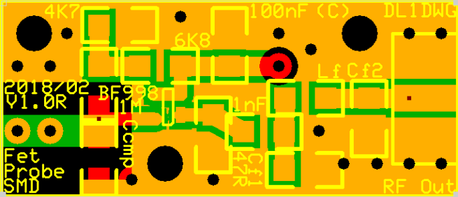
Lacking other ideas, I shrunk the PCB, added a protection diode and an electrolytic cap at the back side of the PCB, and I used two SMD 2.2pF and a 10nH SMD inductor in the output Pi filter. The PCB looks like this:

Hand-soldering this became even more of a challenge; I tried to glue all pads with solder past, add the components and heat it up on a heated plate. This worked, only one leg of the BF998 had to be resoldered by hand.
Characteristics improved somewhat, probably due to the shorter leads at the input. We now have a 3dB corner of ca. 1.4GHz, with all wiggles no more than 1dB up and down.
For mechanical protection I used a heatshrink tube. It also hides my dreadful soldering job from the shocked users eyes :). Funny enough, it also improved frequency response:
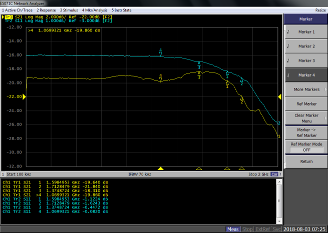
Up to 1.2GHz, we have 19.4 +/- 0.5dB, up to 1.6GHz we stay within +/- 1dB, and the 3dB point is at 1.7GHz. The cost of this homebrew wonder is less than 5€ in total.
Hints for Proper Use of the 1GHz FET Probe
Some advice for properly using this probe is in order, I would think:
- This is no clip-on, or push-on probe, even if such an application would be possible. If you want the frequency response as good as displayed above, the probe must be soldered in with a maximum of ca. 5mm of lead lengths, better even less.
- Dont forget, this is an AC probe with a lower frequency limit of ca. 200kHz.
- The probe is roughly 1:10, as a lot of passive probes.
- The probe works linearly up to input levels of ca. 20dBm.
- The probe can tolerate DC input levels of at least 100V DC due to the PCB gimmick cap used at the input.
- Another word of warning: The probe performance does depend a lot on how it is attached to the circuit to be measured. Even sub 1pF loading is only a few hundred Ohms at high frequencies, every mm of lead length changes frequency response. The output of any “unplanned” probe access is a lot less accurate than impedance matched test ports properly designed into a high-speed circuit. Probes are for qualitative measurements only. Anything more accurate than about 10-20% is just luck.
I did not use a shield so far, because the new PCB prooved to be fairly tolerant against parameter changes coming from surroundings objects. A shield would add some size plus stray capacitance, so I think we can do without for a first try.
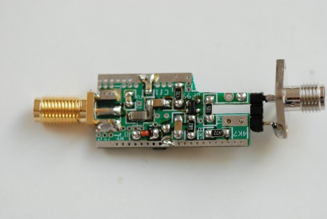
My FET probe now got an “extremely fancy” case so nobody needs to have a look at my dreadful SMD soldering. It now looks like this:

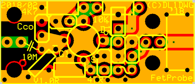
… and the most recent PCB (V1.3) is here:

The broken green areas at the lower left are tuning areas for the coupling capacitance. The ExpressPcb file can be downloaded here:
FETProbeSMDV3R
This probe can be powered from the scope ports of my Keysight scope. I built an AutoProbe adapter for it. It should work with all AutoProbe I equipped scopes (3000 Series upwards).


More info is here:
Click here to See some Info about Using the Keysight AutoProbe Interface in Your Own Projects …
Next Steps
Think about a DC coupled version.
(*) An exception are VNA-calibrated wafer probes using a very well defined geometry and OSL calibration. These are very different from the mobile probes I was talking about. The impedance problem, however, will not be solved by wafer probes either.

Many thanks for this widely detailed project of an active probe used as voltmeter .
As we are a group of radio amateurs on shortwave we started a project of RF power measurement on a well defined impedance of 50 Ohm .
As an extent of this project an RF-voltmeter would be nice .
As your results are quite satisfactory (our limit will be 500 Mhz), and it seems reproducible , we would like to obtain the gerber-files of your last attempt with te BF998 fet .
Even a detailed picture on scale of both sides of the PCB will help us .
With a lot of thanks for your reply .
LikeLike
Hi Willy,
I made this with ExpressPCB (free program, but no Gerbers) but of course you can have the design files if you want ?
They are free for all noncommercial purposes.
Best regards
Wolfgang DL1DWG
LikeLike
Dear Wolfgang thanks for your positive answer . Yes ExpressPCB is known here .
Can you send these design files . It will help us .
I suppose you already have my Email .
Greetings
Willy ON5KN
LikeLike
Hi,
It is any way to get the pcb gerber file?
Regards,
Dan YO8SSV
LikeLike
Hi Dan,
I made them using ExpresPCB, so I have no Gerbers. Do you want the ExpresPCB source file ?
regards, 73
Wolfgang DL1DWG
LikeLike
Hi Wolfgang,
It is ok also with ExpresPCB. Can you send me email with source files?
E-mail yo8ssv@gmail.com. Thanks
Best regards,
Dan YO8SSV
LikeLike
yeah, why not. see PM
LikeLike
Hello Wolfgang!
You really did a wonderful job.
I would greatly appreciate it if you sent me the ExpressPCB source files..
My eMail: wfjr0812@gmail.com
Best regards..
Wilson
LikeLike
Hello, I have put together a SMT version of your probe design where most of the parts are embedded in the PCB between the GND plane and the signal traces.
I would like to share it for your comment.
Its 6mm wide and 21mm long.
LikeLike
Dear Wolfgang, can I add myself to the list of petulants asking for the PCB files of this amazing and very useful project?
73s and many thanks for your invaluable help.
Pino, IK2HEW
LikeLike
Hi OM Pino,
I added the ExpressPCB file on the webpage. Its free for all noncommercial use.
Have fun, 73
Wolfgang DL1DWG
LikeLike
Hi Wolfgang. This is just what I need to work with my nanoVNA. I thought of having a fixed length of 50R coas on output instead of SMA connector. Ant thoughts on this. Also, what size are the SMD components. I have been using EXpress PCB for years, so problem with this side of project.
One lst thing was FR4 board single or dounble sided you used,
73 Laurence G4KLT
LikeLike
Hi Laurence,
IMHO, it is OK to solder a coax directly to the output port instead of the SMA connector. Component sizes are 1206. FR4 was double sided,
because lower part is ground.
73 Wolfgang DL1DWG
LikeLike
Interesting project and very nice writeup. How small of a signal was your probe able to read? It would be great to build a probe that went to -110dBm
LikeLike
Frankly, -110dBm is fairly sporty. This is probably way below noise level. If you assume a 50Ohms source, thats in the microvolts.
LikeLike
I’m looking at building a probe to work with my Spectrum Analyzer where I want to probe the signal chain in a receiver. A passive probe works where relative measurements are possible. The active probe would be a nice improvement with less detrimental effects to the circuit
LikeLike