
To make qualitative noise tests of diodes or transistors over a wide (nulti-decade) current range you have several possibilities:
- use an SMU (e.g., Keysight B2902A) and program a sweep over the range you need
- make your own current source, classic type with a range of measurement resistors, and do about the same the SMU is doing, i.e., step thru the ranges
- or, make a current source with no ranges at all, where you can use a single pot or control voltage to sweep current from some 10nA to some mA, so that a linear pot will result into an exponential current.
The third solution has a lot of charme for fast tests, because all you need is the exponential current source, your DUT and a scope.
Uses of Exponential Current Sources
To my knowledge the most common use of voltage-controlled exponential current sources is the music and synthesizer industry and hobbyism. The current generated is used to drive a VCO, and with an exponential current you can have a linear voltage generating frequencies over several octaves. There are quite some circuit proposals on the next, and the main element is always a somehow compensated double transistor with an op-amp as the exponential current generating element. Common problems are deviations from the ideal exponential behaviour, temperatur dependency and drift. If we look at the audio range, the frequency range is 20Hz to 20kHz, so 1:1000, and this is (VCO linearity assumed) the range of currents to be generated from a voltage span of a few volts. This corrsponds to about 10 octaves (range 2:1), so they often use 1V per octave.
Measurement Requirements, A First Design Idea
We need a lot more range than the music VCO users. We have a few nA (leakage current) up to some mA, say 30nA to 3mA, which is 1:100000. This puts an end to thermistor compensated circuitry. What we really need is
- a tightly matched transistor pair
- temperature regulation, not just compensation
- if possible, all that on the same chip
If we on top want a grounded load and we restrict ourselves to positive output voltages, this means that we need a PNP transistor pair to source the current. What would be very elegant is to use other transistors on the chip to establish and regulate a constant chip temperature, independent on output current and outside temperature.
After some research I found an old PNP/NPN transistor array that looked OK for the job, the CA3096AE. It has the following characteristics:
- 2 matched PNP transistors (up to 35V, 10mA)
- 3 matched NPN transistors (up to 35V, 50mA)
- 200mW per transistor, 125°C maximum junction temperature, 90°C/W thermal resistance, i.e. about 1W of maximum dissipation at room temperature.
The layout of the transistors inside the CA3096AE is shown here:
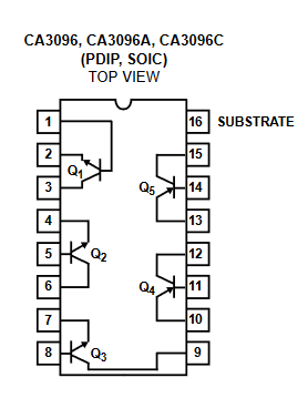
Assuming that the layout on the chip inside resembles the schematics here, I used Q1 and Q3 as heaters and Q2 as the temperature sensor. Q5 is used as the source, and Q4 as the reference. The physical layout of the chip will be analyzed by richies lab, thanks a lot for the effort in advance.
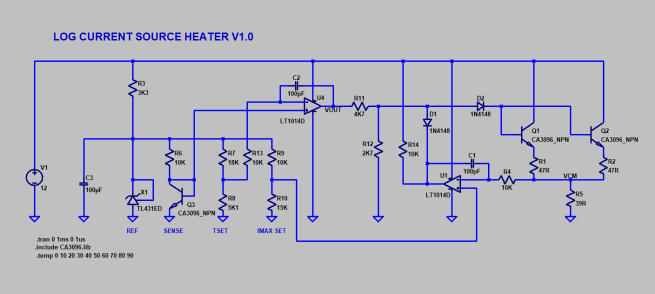
We should go for a moderate but not too small heater power, say 400mW (2 transistor limit). This would set the junction temperature at 25+90*0.4 = 61°C.
The temperature control loop would be closed by an op amp comparing a set voltage with the BE voltage of one of the NPN transistors and driving the other two NPN transistors with an additional current limiter. This simple idea works fine (was also used in some early Jim Williams LT app notes).
OK, this relieves us of any futher temperature compensation efforts. The temperature will stay constant, because its regulated. This also applies if we need to add the dissipation of the output transistor, which can be as large as the maximum output voltage (here 25V) multiplied with the maximum output current (say, 5mA). This will give 125mW, so the heater power will be reduced by this amount and the temperature will still stay constant.
The circuit can be seen here:
The Exponentiation Circuit
This uses, in principle, the exponential relation between collector current and base voltage. So what we need is some sort of range setting circuitry that defines the lower and upper limits of the base voltage, and a linear multiturn pot that selects any voltage in this range. The circuit is shown here:
The 2N3906 transistors are the two PNPs of the CA3096AE, where the PNP model seems to be flawed. It works nevertheless.
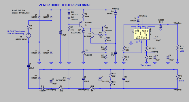
Power Supply
I split the supplies of the heater portion and the exponentiator. The heater part uses a supply voltage of 20V, derived from the main 30V main supply. The heater supply voltage is chosen to set the maximum heater transistor dissipation (In my case, I am running the transistors at ca, 250mW, which is a bit more than allowed, but the total chip dissipation is way below 1W. So far no problems). The exponentiator part uses a 30V supply wih an interal virtual ground at 25V. I did this to get a usable compliance range for the output DUTs like Zener diodes with 12V, e.g. The virtual ground is created by an op-amp. The ranges for the base voltage of the exponentiation PNP transistors are around the virtual ground; to derive them from the 30V operating voltage I made a chain of two resistors and between them 2 TL431A based shunt regulators centered around the virtual gound and divided to the ranges needed. The schematics is here:
First Results
Worked very fine, I must say. I got a range of 5nA (!) minimum (this is the leakage current, dont forget we are also running at an elevated temperature) and 5mA maximum from 10 turns of the precision pot, all measured on a Keysight 3458A This is covering 6 decades, quite a lot more than expected.
The innards of the unit are shown here:

At the top we have the double filtered power inlet and power switch, plus a slighlty redimensioned power supply from the Zener diode tester. Here we dont need the negative 4V supply, and 30V are enough, but we need up to 50mA of supply current because of the heaters. Its doubly stablized by a TL431 based pregulator giving 33Vs, and a LM723 regulator for the 30V. Current limiting is done on the TL431 part of the circuit. The PARD of this is below 300uVpp.
The PCB at the bottom is the exponentiator part. The artificial ground rail splitter (LT1013) sits on top left, the LM324 to the lower left does the voltage adjustments for the multiturn pot so that the range boundaries are what we need (5nA to 5mA). The CA3096AE transistor array sits in the center, and the LT1013 at the right does the temperature control and the heater current limiting.
Setting this thing up is done in the following way:
- First, set the temp pot at a voltage way above a reasonable room temperature diode voltage drop (say, at 1V). This turns the heater completely off.
- Next, measure Vbe of the temperature sensing transistor/diode at room temperature. I got a value of 0.62V.
- Now we have to decide about the desired chip temperature. Lets assume we want to be 40°C above ambient, so the expected voltage drop would be roughly 2,5mV*40 around 100mV. Now set the temp pot to a value where the temperature set voltage is 0.52V. This should take care of a constant chip temperature, independent of the dissipation of the output PNP transistor. You can check this by blowing some air at the CA3096AE and see the heater current react accordingly.
- The current range setting is next. Attach the 10-turn pot and set it to its minimum and maximum value. The extremes can be trimmed by the two pots on the left side. My choice was 5nA to 5mA, but a little bit more would have been possible.
- Done!
After changing the current setting, the circuit needs a few seconds to fully settle due to the thermal time constant. One stabilized the current is very stable with almost no drift – thanks to the constant temperature and the well stabilized power supply.
Next Steps
What would be nice if the circuit would become SCPI controllable, or at least with an external control voltage between, say, 0 and 5V for 5nA to 5mA.
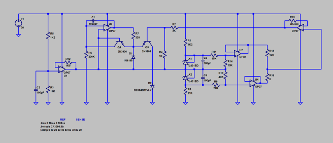
A Voltage Controlled Exponential Current Source
The circuit here more or less works like the manual one, except that the current can be set by a ground referenced control voltage. The schematic is shown below:

The control voltage is shown at the bottom left. What we would like to see is a good log linearity from some nanoamperes to as far we can get before beta degradation sets in. This is a compromise between leakage, high current effects and how much degradation from the ideal log curve you are willing to tolerate. The setting I made looked like this:

Current can be controlled up to 1mA, but linearity starts do fail around 50uA. The error plots show this:

Below 30uA the error stays well with 10%. At the low end, we start at 15nA, so we end up with a 1:2000 range with less than 10% error. For something without feedback this is OK.
What this unit also needed was a beefier power supply. We needed 35V at 50-70mA, and 5V at a few ten mA. The old trick to derive the negative voltage from a single transformer did not work anymore, so a small, separate transformer was used to provide the negative bias. This worked fine. The schematics is here:

The voltage controlled version also needed a larger case. The innards can be seen here:

The top has the line input filter and the enlarged power supply for +35V and -5V, the bottom has the current source with voltage input and current output on BNCs. The boxed unit looks like this:

